Wednesday, October 2, 2019

Shooter game in silicon: inside the AY-3-8605 chip


Once again, another dedicated video game chip has been digitized and simulated! That makes a total of three dedicated videogame integrated circuits. This time it's the AY-3-8605 "Sea Battle" chip in a browser simulation. In this post I'll show a high-level overview of how it works, as well as share a few interesting things I found while working on emulating it. Let's dive in!

Background & Gameplay


PC-505 cartridges were sold under names such as Submarine, Sea Battle, Bataille Naval. (source/more info)
The AY-3-8605 was part of General Instrument's 8600-series "economy" line of game circuits. These chips provided the game logic to the numerous "PC-50X" compatible video game consoles, which were produced en masse in the late 1970s. These systems could play different games by swapping out cartridges containing different custom circuitry, such as the PC-505 cart which contains the focus of this post. Despite having interchangeable cartridges, these weren't true re-programmable systems like the later Atari 2600. The console only contained
A PC-50X compatible (Multicherry)
the power supply, TV interface circuitry, and controls while all game logic was located in the cartridges.


The gameplay and graphics are very simple, as they're generated by dedicated circuitry. One player uses their joystick to control a submarine while the other controls a destroyer ship. Just shoot your opponent with torpedoes/depth charges while avoiding their attacks. A few variations on this concept were presented as entirely different "games", such as a single player mode versus a simple AI, variants with an autonomous cargo ship to defend, or versions played with spaceships.


Die photos


The picture below is a photo of the silicon surface of the sea battle chip. Like the previous game chips I've looked at, this one was decapped and photographed by Sean Riddle over a year ago. The single metal interconnect layer is easily visible as lighter areas, while the other layers are mostly hidden beneath this. The polysilicon, vias, and diffusion traces are much easier to see and highlight in this picture, of the surface after the metal was removed with additional chemicals.


It took me about a month to trace out the different components using a paint program. This was then processed into a digital model of the circuitry (a netlist), which can be plugged into a simulator like the visual6502's. After a little bit of debugging it successfully generated screenshots of the original game.

The control panel (top), virtual chip (left), and video output (right)

You can check out the AY-3-8605 simulation here. Keep in mind that it's only meant for testing & debugging so I didn't bother to clean it up or make it user-friendly. Note: the ships won't show up unless you toggle the reset signal "on" for a hundred or so cycles.


Each green square is a single NMOS transistor, there are 2777 in total. If the metal on top of the gate is charged, electricity is allowed to flow through the source and drain below it, otherwise it's an insulator (this simulation is all-digital, as the chip is entirely digital except for some Schmitt triggers.) Connecting transistors together is accomplished through a single metal layer (grey), and N-doped silicon (blue.) It may seem rather complex, but it's multiple orders of magnitude simpler than modern CPUs which contain billions of transistors and well over a dozen metal layers.

Input/Output


Around the edges of the die are 27 rectangular pads which function as input/output. In a physical chip these would be connected through tiny bond wires to the package pins. The ground and Vcc (power) pins, on the middle of the sides, branch throughout the chip to support the logic inside. At the bottom is the 3.57954Mhz clock input pin which advances the circuitry. This is the NTSC colorburst frequency standard, used as a baseline for many old electronics. Note: this sample is actually a PAL-compatible chip, not NTSC.

The two directional control pins are in the upper-right corner. These are tri-state pins with Schmitt triggers, they regularly drain an external capacitor and measure the time it takes to charge, which is based on the rotation of the potentiometers in the controls. This may seem unnecessarily complex as the ships only have one possible speed, however it's necessary as the chip had to be compatible with the same controllers meant for pong-like games.

Four pins are responsible for the four different sound effects. The sonar and explosion effects have much larger driver transistors, presumably to increase their output current. There are a total of seven pins dedicated to video output: sync, colorburst location, the four possible colors (L-video, R-video, Background, Blanking), and hue. Another five pins are dedicated to game selection; three sense and two strobe, which multiplex six game select buttons.

A huge driver transistor to the right of a much smaller counterpart


Major features


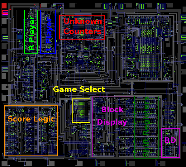
Several major functional blocks are immediately visible. In the lower left of the die is a circuit that divides the 3.57954Mhz clock by two, and drives two alternating clock signals throughout the chip. Directly to the left of that is the horizontal counter, situated under its vertical counterpart. These use the steady clock to produce television sync signals, as well as determine the location of stationary game objects (scores, etc) These circuits are very similar to counterparts in the chips covered in previous posts.

The score memory logic (top) and drawing (bottom)
The score logic (upper-left) seems to be identical to its counterpart in the AY-3-8606. The designers at GI probably reused this design in most of their dedicated game circuits.


About a 5th of the chip is taken up by seven counters in the lower-right quarter of the chip. These counters store the position of the 5 game objects (cargo ship, destroyer, sub, torpedo, depth charge.) Five of the counters store the horizontal positions, while two store the vertical position of the projectiles. As all three of the ships never move up or down, their drawing logic is tied to the vertical sync counter rather than separate counters. These types of counters are called "slipping" or "jumping" counters. They constantly advance at the same rate as their sync circuitry counterparts (pun intended.) Once a field, they may either slip behind or jump ahead based on player input or game logic. This causes them to become slightly offset from the sync counters, which translates into a visual offset on-screen. Repeated slipping results in smooth motion.

Telling the vertical counters apart from the horizontal ones is easy (due to transistor size & clock signal.) Figuring out which game objects correspond to which counters isn't as easy based on static pictures alone. However, it's possible to see the different counters in action via the simulation. Watching the counters at work allows us to figure out which ones correspond to which ships/projectiles, as shown in the diagram below.


A few other logic blocks have been identified. At the top middle is a 5-stage ripple counter which turns the 15625 Hz horizontal scan frequency into 477 Hz, used by some of the sound effects. To the right of that is a lookup table and shift register which generate the different ship graphics, more on this later.

When hit, the ships flash their opponent's color
The four possible game colors come out on four separate pins but the colors of the ships can change during gameplay. Two logic blocks are responsible for managing colors. The first one decides if objects should be drawn in the left player's color, the right player's color, or not at all. The other rearranges the palette during the space games, and ensures that exactly one color pin is active at a given time. The colors are also dependent on external circuitry (such as an AY-3-8615 chip) which can itself be dependent on the selected game. One other note: the hue pin's affect on color is used to show contrast between the air and underwater.


Slow game logic


While debugging the simulation, I noticed that the submarine wouldn't move. After a little investigation it turned out that the sub's movement was simply disabled for a dozen or so frames after reset. The simulation wasn't being run long enough to enable movement. This and other "slow" behavior such as the cargo ship's movement, the sonar ping, blinking & loss of movement upon being hit, etc are controlled by the "slow" counter. This advances every 8 fields (~1/6th of a second) and takes longer to cycle around. Behavior like this is almost impossible to discern from footage, and would have never been noticed without die analysis.

To properly test the submarine's movement, I tied a checkbox (labeled Turbo) to the slow game logic's clock signal. Clicking it a dozen or so times advanced the slow counter enough to enable movement, much faster than running the sim normally for several fields. Not the most elegant solution, but it was easy to implement.

Ship generation logic


Amazingly detailed spaceships
There's one part of the die that I want to share in a little more detail. The ship graphics are a step up in complexity compared to the simplistic squares in the previous games covered here. Only five different graphics are possible though, one for each of the three ships and two for the two spaceships.

The circuitry to generate these stunning visuals takes up a non-trivial area of the die in the upper-right corner. The graphics are so simple that they don't use a ROM in the traditional sense, rather the shapes of the ships are decided by a look-up-table (green box.) A signal indicating which layer of the graphic is being drawn, along with a signal indicating if a space game is playing, travel into the look-up-table. Fourteen different signals are generated by this table (multiple active at once.) These mesh with three more signals determined by which ship is being drawn, before flowing into the output shift register.

The output shift register consists of twelve segments and six inputs. It's mirrored such that one signal controls the middle two elements, while one controls the ends, while the remaining four control the pairs in between. In short this means the look-up-table only has to hold the information to draw one half of the ship, which is then mirrored. This shift register is enabled whenever the counter of the currently drawn ship reaches a jump point.

The output of the shift register is put onto one of three wires (one per ship) which go into the first color matrix and collision detection logic. The output of the shift register can also be forced into an active state by use of the test pin, which results in horizontal bars like those in this screenshot. I suspect that the reasoning for this is to make any sort of aiming unnecessary when testing the collision logic during quality control.
Output of the chip when the test pin is active

Conclusion


The AY-3-8605 is a relic from a bygone era where video games were designed by electrical engineers rather than programmers or artists. The work done here will insure it will be still playable in the distant future when functional units become scarce.

A few things need to be done before it's playable. As the transistor-by-transistor simulation is too slow, the netlist will need to be converted into more abstract verilog using DLAET. That can then be ported to the MiSTer platform or converted into a software emulation. I'll also have to figure out the best way to re-create the behavior of the external analog sound circuitry.

Before that happens the AY-3-8500 has to be ported to the MiSTer. I've got it to run as a working core, however there are still issues with reliability which prevent it from being playable. Once I figure out a solution to that problem, I'll release the core and share some other things I've been working on since last time.

You can follow me on Twitter for the latest news related to the project. Also feel free to ask questions below. Have a spooky October everyone!

Friday, July 5, 2019

Playable emulation, and more!


It's July already! 2019 is half over! My last progress update was several months ago back in March. I meant to post an earlier update, but I waited until I had playable pong to show and share. Yes, I finally have a complete verilog description based on die photos of the AY-3-8500, and it can be run on a physical FPGA. Along with that, I have other exciting news related to the project. Let's get started.

First, the recap. For the past few months I've been working on creating accurate emulations of 1st generation video game systems. These games may be deceptively simple, a large chunk of them are just clones of pong, but the
game logic is burned into specialized integrated circuits. As detailed documentation is scarce, I've been recreating their behavior by converting photos of the internal circuitry into a verilog description of the logic circuits.

The first chip being emulated is the AY-3-8500 "Pong on a chip" circuit. It formed the heart of over 200 different types of pong consoles produced in the later 1970s and early '80s, which were produced in the millions. As you'd expect, it contains the digital circuitry to play a few different pong-like games (plus two games with light guns) on a home TV set.

Beep-Bop-Beep


Above is a video I recorded of the AY-3-8500 being emulated on a FPGA chip. The paddles move, the ball bounces, and the score increases each time a goal is achieved. Grounding certain pins selects the different games, while others modify the gameplay slightly, just like on the real thing. Everything has been tested except for the rifle circuits, as I didn't setup the external hardware needed to support a light gun.

Overall it accurately recreates the behavior of a real AY-3-8500 chip. The only major difference is that the ball doesn't always hit the paddles when I want it to; this is probably caused by the bad controls I used and definitely not due to lack of skill or anything like that.

Screenshot of nextpnr showing the placed & routed components

You can find the source files here The folder contains the verilog description of the AY-3-8500-1, a top.v file specific for the tinyFPGA BX, and a compiled bitstream. If you have a tinyFPGA board, or another FPGA with the necessary tools, then you should be able to play it yourself (note: there are issues with the place & route, see below). If not, you'll have to wait until it is ported to a MiSTer core or made into a software emulation.

Next things tor the AY-3-8500


Although the vast majority of it completed, some work related to the AY-3-8500 still needs to be done. First off, the verilog has about a dozen manual patches in it which need to be worked into DLAET. There is also a decent possibility that an error or two made it into the verilog without being noticed or patched. Eventually DLAET's output should be as accurate as the FPGA allows without any patching.


There are also problems concerning the design's reliability upon being placed and routed. As I've talked about before, there are many "nasty tricks" which hardware designers used long ago which are difficult to translate to modern hardware. I've written code to recognize and handle most examples of these, however the verilog still breaks a few hardware design "no-nos". Because of this, a large number of generated bitstreams (the file that is loaded onto the FPGA) will work incorrectly. This can be overcome by changing the random seed for the place & route algorithm until it works correctly, a little tedious, but OK in lieu of a better solution for the time being.
 
The breadboard game setup I used isn't very convenient, especially with the composite plugs dangling off of it. I also used a pair of cheap potentiometers from an Arduino kit. Because of that, non-recommended values, and unsoldered connections, the paddles jitter like crazy. Not a long term solution. As said before, I'm going to port it to the DE-10 board which runs the MiSTer project. This should be a fairly straightforward process, and will make playing it MUCH easier.
The DE-10 Nano board that MiSTer uses.
Software only emulation is also straightforward. Originally when I started writing my netlist processor (DLAET), It was going to output C++ code. Later I learned about Verilator which does much of the work for me once the netlist has been converted into verilog The verilog (actually an older version of it) was already successfully converted into a C++ file. C code to display the signals and poll user inputs will need to be written to make the simulated chip playable. After doing some thinking I decided that the best way to proceed would be to create a standalone emulator, then porting the code over to MAME (possibly a fork). I should have screenshots or source code of a software emulator not too far in the future.

Sea battle!


Those of you who haven't been following along may wonder why is this such a big deal, and why did it take months to complete something so simple? After all, pong is a common project for people learning FPGAs. The AY-3-8500 has also been reproduced before because very detailed documentation is available. The importance of this implementation is that the process developed is based on die photos instead of datasheets/observed behavior, and much of it is done automatically. The process and tools pioneered here can, will, and are being used on other game chips with less documentation. In fact, another chip has been simulated in the visual6502 engine since last time.
2777 Simulated transistors
The AY-3-8605 chip (aka Naval Battle, Sea Battle, Warfare, Bataille Navale) generated a fairly unique skill game pitting (very blocky) ships against a submarine, or (also blocky) spaceships against one another. Games were either two-player or single-player versus an extremely basic AI. Here's a video of an original system in action.

A screenshot generated from the JS simulation


It took about a month to highlight the images of the chip, which I started doing in April. Once that was done, I spent a few days in mid-May correcting errors in the highlighting and learning a little about how the chip works. Just like the Wipeout chip had a post detailing some of it's internal workings after it was simulated, the same will be done for the AY-3-8605. Its circuitry is somewhat different from the two chips covered so far because it's not a moving ball based game.
So when will it actually be playable? As said before, the AY-3-8500 is pioneering the die photo -> netlist -> emulation process. Most of the work needed to turn the JavaScript simulations into playable FPGA cores has already been done, however because of shortcuts and edge cases the '06 and '05 netlists can't run through DLAET fully yet. I've already spent a few days working on this issue and will work on it more now that the AY-3-8500 has reached the playable stage.

Even more chips


What else is on the journey to emulation? Only three more game chips have been photographed but not highlighted: the AY-3-8600 (improved AY-3-8500), the MM57105 (a competitor pong chip), and the MPS7600 (responsible for these games.) The MPS7600 and SP0256 sound chip are comparatively quite complex, so I want to gain experience and improve debugging tools on the less complex chips first. And since the only chips I've done so far were made by General Instruments, I decided that the MM57105 will be the next target for highlighting. I haven't had time to start highlighting due to my summer schedule, but I'll pick it up again sometime soon. Also, as I've said before, highlighting isn't a difficult process and you can contribute if you want to help.
The MM57105's surface

Other chips are on the way to be decapped and photographed soon. David Viens has collected a few more specimens to be sent to the acid bath. The ICs he has acquired are the AY-3-8603 (a vertically scrolling racing game), the AY-3-8607 (several games to be played with a light gun), the AY-3-8610 (slightly more features than the AY-3-8600), and the AY-3-8765 (a one-chip implementation of Atari's stunt cycle arcade game.

That's plenty of new chips already, but thanks to donations from some of my readers, I purchased some vintage 1st generation game systems online. These systems will be gutted to remove the custom chips for decapping. Another very important thing that can be done is document the PCBs to figure out the pinouts, as many game chips did not have public documentation like the AY-3-XXXX ones do. I'll also get some good pictures of the internals/externals as well as play footage if none exists so far. Last thing I plan to do before removing the chips is figure out how to composite mod them, useful information for anyone wanting to improve video quality on their own systems.

So far I've acquired four different systems. First is Atari's video pinball dedicated system. You may have heard of video pinball for the 2600, but you may not know that they made a system (and thus a chip) hardwired to play electronic pinball as well as Breakout and a basketball game. In many ways the dedicated version is better than the 2600 version. Sometime I'll make a blog post showing the internals, as well as how to composite mod it (composite mod has been completed.)

Such detailed graphics! (for 1977)

Next up are the Coleco Telstar Combat! and Phillips Odyssey 2100. Combat! uses the AY-3-8700 to play two tank battle games, like Atari/Kee's Tank arcades or the 2600 Combat cartridge. Matches were between two players or against a simple "robot" mode. The Odyssey 2100 used the MM57186 chip to play a few color games based on the ball & paddle concept. Actually I didn't get the Odyssey, I got a sample of the chip by itself (the chip wasn't exclusive to the Odyssey.)

A PNG of the CTVG's PCB (say that three times fast), showing the M58816P custom chip
The purchase I'm most excited about wasn't sold here in the USA, despite it's maker later selling tens of millions of other videogame consoles worldwide. It's the Color TV game 15, Nintendo's first console! Technically the TV game 6 (probably) came out before it, however they used the same custom game chip so emulating one will emulate the other. Despite holding such historical significance, no attempts at emulation have been made (other than a very inaccurate re-creation.) Time to change that. First though, I want to try out a guess I have on how to composite mod it.

A highly inaccurate re-creation of the Color TV game made by Nintendo
Hopefully good die photos will show up after these chips are shipped off. I say hopefully because, surprising as it may seem, dissolving microscopic circuits in boiling acids is not a completely predictable process. There's a decent chance that something will prevent usable images from being obtained. You can see an example a few paragraphs back; a bit of the MM57105 has broken off in the lower-right of the die (this isn't severe enough to require new photos though.)

I took several pictures already of the consoles, all of the good ones have been dumped here. They're all public domain, so use them for whatever you want (provided it's not illegal.) I'm not a professional, but I tried to get some good-looking shots.

Wrap Up


This project took a lot of time and work, so it's good to see playable results from it. This project wasn't me alone though. I want to thank Sean Riddle for decapping and photographing the AY-3-8500, David Viens for sending the other game chips his way, and the people who gave me money to acquire even more specimens. Also thanks to Greg Davill and Adam Courchesne for answering some verilog-related questions.

Lastly, thanks to the people who organized Latch-Up. For those who don't know, Latch-Up is a open source hardware conference that ran for the first time in May. I gave a talk on this project, met new people, and learned a lot. Hopefully next year will be even better!

There are a lot of different things to work on. I'll keep you all updated on what's happening on this blog, so be sure to check it every once and a while. You can also follow me on Twitter for smaller updates and pictures of progress. Now that one chip has been converted into a FPGA, the rest of 2019 is sure to bring some great things!

Thursday, March 28, 2019

The AY-3-8606, another successfully simulated circuit


Since I began this blog it has focused on preservation of the AY-3-8500 "Pong on a chip" circuit (with one exception.) As has been said before, the tools and experience developed to emulate the AY-3-8500 can be used on other discrete circuits from the time period. The AY-3-8606 "Wipeout" game has now been simulated using said tools and experience, just like the '8500 was in August, and it took under two months to do so. This post describes the work done so far, and also documents some of its internals.

How to emulate discrete integrated circuits


I've talked about the process involved in past posts, here are the steps laid out again.

1. Obtain circuit specimens
2. Decap, photograph, and stitch images
3. Highlight images
4. Process images and correct errors
5. Simulate circuit in JavaScript, correct more errors
6. Run DLAET to abstract netlist into Verilog
7. Port to FPGA
8. Use Verilator to emulate circuit in MAME

At this moment, the AY-3-8606 is at step 5 and the AY-3-8500 is currently pioneering step 7. Thanks to Sean Riddle for undertaking steps one and two, which resulted in the images below. Note: All die photos on this post come from Sean Riddle under CC-BY-4.0.

You can check out the JavaScript simulation here. The simulation is purely for debugging purposes, so I haven't made much of an effort to make it user friendly. The files involved with the process are available here.

First impressions


The AY-3-8606 was part of General Instruments 86XX "economy" game system circuits. Like the earlier AY-3-8500, GI sold these chips to anyone wanting to build and sell systems using them. Many almost identical consoles were produced using the schematics and screenshots found in the catalog (page 460), these are now referred to as PC50x systems. The console contains the support circuitry, controls, color chip, modulator, speaker, etc while the interchangeable cartridges contain the unique game chips.

A standard PC50x system (pong-story)


The PC506 game carts went by "Wipeout", "Wipe-off", "Destruction Game", "Brix Game", or "Jeux de destruction" and contained an AY-3-8606 with it's pins mapped to the cartridge connector. 10 game variants, some two-player, can be selected using the console's buttons. Additionally, three switches could adjust the bat size, ball size, and speed of the game. Below is a table comparing it to the earlier AY-3-8500. It's a bit more complex, but not by much.


AY-3-8500 (NTSC) AY-3-8606 (NTSC)
Transistors 2318 2975
Nodes 973 1633
Polygons 10292 12435
Input clock ~2Mhz 3.579545Mhz


The AY-3-8606's surface.


Above is an image of the decapped chip's surface. There are a few noteworthy features immediately visible. Three wafer test circuits are present on the edges of the die. The text "© 1978 G.I. CORP." fills an empty spot in the upper-left. Nearby that is a collection of numbers written using different layers. Lastly "80-80395" appears in the bottom-right. None of these features affect the game logic, so highlighting them isn't necessary.

There is a repeating structure near the bottom right. This stores the state of the blocks inside six shift registers, corresponding to six rows of blocks. Interestingly, there are 10 segments per shift register, but only 8 blocks per row. More on this later.

Fixing errors


A high resolution look
The 2048*1810 images I used are clear enough to discern almost all features on the chip. The indistinct spots are resolved using the high-resolution images. Nevertheless little errors are made and need to be found. Four errors had to be fixed before my image processor would succeed. After it did the debug images then revealed over two dozen other errors. After a little more debugging work and modification to the virtual TV code, the JavaScript simulation produced the image below.


The generated image, along with the datasheet's rendering of game #9

It works! ...but not correctly. It looked like game #9 from the catalog, except some of the bricks were on the wrong side, the scores were vertical lines, and the bricks overlapped the top bounds. Time for more debugging!

Unlike some other chips, PC50x series games use strobed signals to read up to 10 different game select buttons with only 7 pins. It seemed that without external buttons the circuitry was changing to game #10 partway through a screen, explaining the misplaced bricks. I wrote a little code to simulate the external buttons via a checkbox, which fixed this issue. Because of this strobing the 8606 will probably exhibit odd behavior whenever multiple buttons are pressed, I haven't experimented with it though.

After selecting one of the other games, I saw that 9 columns of blocks appeared instead of 8! A close look at the shift registers revealed that they held 10 columns of blocks. The 10th column, which is off the right side of the playfield, is always reset to empty. The 5th column (middle) is reset to empty/full based on the game selection logic.

Take a look at this captured footage (skip to 4:14.) In game #9 the wall appears to be 9 layers thick (this confirms the catalog's screenshot.) So at least one game mode uses the middle column. It turns out that activating the reset pin (which the simulation does before loading) can only reset the blocks when the scanline is in a certain region. If you turn it on for longer it will correctly reset the blocks. This means that switching from game #9 to another one without hitting reset will leave blocks in the middle column, doing the opposite will create a gap in the middle of the wall. Also, the footage seems to suggest that the blocks do overlap the top boundary in real hardware. I don't have a physical console to confirm that this is the case, but the fact that little details like these are preserved is pretty impressive in terms of emulation accuracy.

This was causing the vertical lines. Can you see what's wrong?
The right player's paddle and score were missing (although I'd personally be fine competing against someone with no paddle), and the left player's score was still vertical lines. After a little more error hunting the output looked correct for all possible games. Odds are there is still an error or two present, but most of the circuit is correct.


Game 7

Looking at the circuits


I've explained some of the AY-3-8500's circuitry in great detail. My current focus is emulation, so I won't do the same thing for the AY-3-8606. Here's a short overview of different components based on what I learned while debugging it.

The 3.579545Mhz clock signal comes in through the aptly named clock pin at the top. This is halved and used to drive two alternating clock signals throughout the chip. 3.579545Mhz is the NTSC colorburst frequency, crystal oscillators at this frequency were mass produced for TV sets and thus made inexpensive by economies of scale. The non-NTSC 86XX variants, many later systems and even non-television chips used this standard frequency as a clock source or reference.


Next to the clock divider + driver is the horizontal and vertical control signals, just like in the AY-3-8500. The shift register is a little smaller though. All of the shift registers in the 8606 are more compact because they use capacitor-capacitor segments, unlike the AY-3-8500 which uses mostly capacitor-latch segments.


To the left of that is another horizontal+vertical counter pair. What this one does is a mystery to me, although I''m guessing it's part of the ball circuitry. Past those are the two paddle counters, one for each player.

In the lower-left is the score counter/display logic. It seems almost identical to the score areas on the 8600 and 8605 die photos. Another area of interest is the center where a game select PLA resides.


Next Up


The next step for the AY-3-8606 is to convert it to Verilog using DLAET. That will have to wait until I get the AY-3-8500 fully working on an FPGA. In the meantime, I'll be working on highlighting another chip.

You can contribute by highlighting! It's visual identification, not necessarily hard, it just takes a lot of time. The AY-3-8606 took over a month to highlight, while processing and error hunting took less than a week. Highlighting doesn't require much focus, so I worked on it whenever I needed to listen to something else. Shout-out to all the people who let me work on a laptop wherever one does not usually work on a laptop, you are preserving games you never even heard of!

What chips are next? plgDavid of the MAME team is sending off some chips to be decapped. He has the PAL variants of the 8603 (road race), 8607 (light gun games), and 8610 (improved 8600.) Hopefully useful die shots will show up sometime soon. If you have circuit specimens or the consoles that contain them (nonfunctional included) and wish to donate, I'll help with finding someone to decap them. I'm particularly eager to get die shots of Atari's chips, and the ones in Nintendo's Color-TV game series.

In the meantime, there are four existing die photos I'm looking at for emulation. First up is the 8600 (NTSC variant) which is pretty much an upgraded AY-3-8500 with more games and bidirectional movement. Second is the 8605 (PAL variant) submarine/warfare chip. Third is the MM57105, National Semiconductor's competitor to the AY-3-8500. It could play its games in COLOR (without a support chip.)

Die surface of the TMC0280

The last game chip to have been decapped as of 3/2019 is the MPS-7600, from the Coleco Telstar Arcade cart #1. I'm not doing this one anytime soon due to lack of any documentation, and also because its much more complex than what I've done so far (it has a custom microcontroller inside.) The fourth chip I'm thinking of emulating is the TMC0280. Never heard of it? How about the Speak & Spell? The TMC0280 is the voice decompression/synthesis engine inside it. It has a lot of transistors, but many of those are part of repeating arrays.

So which one to work on next? Comment below if you have a preference, or try highlighting one yourself. I'm leaning towards the AY-3-8605 because its a fairly unique game.

Two other things: first, I'm in the process of setting up a Patreon account for anyone wanting to contribute monetarily (all files and posts will still be public.) EDIT: here it is! Second, I'm going to be giving a talk at Latchup conference in Portland (Oregon) come May. Stop by if you're one of the 0.0086% of people around there. Anyway, my next post should be on the current/future progress of FPGA porting, so stay tuned (to channel 3 or 4. ;)

I ran the simulation for 10 million cycles while writing this (~1.4 seconds) The ball clearly moves, bounces and destroys blocks. (There was an error in the score logic)

Tuesday, March 5, 2019

"Febuary" Progress Update

I said I'd have another progress update in February, so here it is! I've made great progress on multiple fronts, and run into a few ongoing challenges along the way. For those uninitiated, I'm working on creating emulations of late-70's era discrete video game chips. You can find a more in-depth review in my last update.

Its funny to think how this project, which was originally just reverse-engineering the AY-3-8500, would have been completed months ago had it not been for me moving the goalposts. Here are my current long-term goals:

1. Create a FPGA emulation of the AY-3-8500(-1) for a FPGA system such as MiSTer

2. Make a software-only emulation of the AY-3-8500(-1) in MAME

3. Use the experience/tools gained to repeat the process for as many of the other 2 dozen+ discrete game chips out there

Lets take a look at what's been accomplished over the last month and a half.

FPGA emulation


As explained before, I've been working on creating a program to reverse-synthesize the low-level netlist of the AY-3-8500-1 chip into more abstract components which would be eventually converted into a Verilog circuit description file. This file can be used to configure a FPGA, a chip which contains mesh of re-programmable logic blocks. Current testing is done on a tinyFPGA-BX board, although I'll probably port it to something else (more on that later.)

The 972 nodes which make up the AY-3-8500 were reduced to 360 by the last update, it's now down to 318. That number is not very important, it just shows the reductions that are possible through reverse-synthesis. Those 318 components create a Verilog file which, after one or two manual patches, is programmed into the FPGA board via USB. Connecting the circuitry to a TV give us...


Squash, along with a visitor
...a game of "handicap"! Unfortunately it doesn't play or show the scores yet, as explained below. All of the virtual chip's pins have been mapped to the board's pins so attaching a grounded jumper to pin 4 will display a squash game. Grounding pin 5 will result in a tennis game, pin 6 Soccer, etc...
Tennis appearing sharp, albeit less retro on a digital TV


Below is the breadboard setup, on the left is the tinyFPGA board, andnext to it is a reset button. To the right of that is a 2x quad-OR gate, and past that  is a resistor network and controller circuits. The circuitry is almost exactly like the diagram in the manual, just with different value components and a direct composite connection instead of a RF-modulator. I goofed up and ordered a non breadboard-friendly RCA plug, which is why the connector dangles off the board (its connected to the two wires leaving the right side of the picture.)


Nothing a little soldering won't fix
As you can see, the current setup is not at all user-friendly, given it's composite-only output, support circuity, and cat-vulnerable mess of wires. This is because, the FPGA is currently emulating the AY-3-8500 and nothing else. If we ignore the 4 unchangeable pins and the voltage difference, the configured board can be pin-compatible with the original!

I'm planning on porting it to a core for the MiSTer FPGA retrogaming system, once I get a hold of a DE-10 Nano board to test it. This will eliminate the support circuitry and allow for VGA or HDMI output, among other things.


Challenges


The paddle inputs are currently not working correctly due to either an incorrectly configured pin or because the board is hooked up to wrong value potentiometers. The internal paddle circuitry is working as expected though (I tested this by adding code to trigger the pins based on the vertical counter, which is why the paddles appear above.)

The reason why the score display/playing capabilities don't work yet is due to a more complex problem. Almost all modern digital logic is synchronous, meaning registers only update when the clock signal does. Because signals with different latencies must wait for the synchronized clock, they won't trigger race conditions as long as the clock is no faster than the slowest signal.

The AY-3-8500 uses some more complex asynchronous logic along with "nasty tricks" such as pulse-on-edge circuits and latches which make porting to modern hardware difficult. Note that its difficult but not impossible. Working asynchronous logic can be created, in fact its an area of active research in semiconductor design. The problem is software tools can't handle it's unique needs yet, and the FPGA hardware blocks are built with synchronous logic in mind.

A "nasty" on-edge-pulse circuit

I believe this is possible though. Latches can be made inside FPGAs by combining many logic blocks. This is inefficient on resources, however the FPGA I'm using can already hold multiple copies of the AY-3-8500. Many of the "nasty tricks" can (and have been) eliminated during processing while keeping behavior identical. Lastly the AY-3-8500 only needs to run at a snailish 2Mhz which eliminates some of the problems associated with asynchronous logic.

That doesn't mean there won't be issues. For example, the logic which loads the score shift register is somehow being affected by component placement, despite the fact that it loads synchronously with ample time for signal propagation! This has had me stumped for a while. Hopefully changing the build tools from arachne-pnr to nextpnr will fix or offer insight into this issue. Also, I would like to thank David Shah and Claire Wolf (two of the developers) for taking the time to answer my (possibly bothersome) questions on these issues.

Another challenge: SABOTAGE!

Other Advancements


No software-emulation specific work has been done yet, although I have some good news regarding speed. I simulated the circuitry in a program called Icarus and measured the execution speed at 1/9th real world speed. This would only allow for playable emulation on PCs in the "overclocked i9 with water cooling" range, thankfully there are much faster methods of circuit simulation. Icarus runs by interpreting intermediate files, while Verilator works by converting the source into very high speed C++ code. It claims improvements of 100X, which seem reasonable given the actual work involved (I estimated that 75% of the AY-3-8500 cycles consist of merely incrementing two counters.) Once bugs have been ironed out via FPGA testing, I should be able to Verilator-ify the file and write a driver to interface it to MAME.

What about the other chips? Another one is currently in the process of being highlighted. Its the AY-3-8606-1 "Wipeout" chip which is a weird cross between pong and breakout. Unlike the well-documented AY-3-8500, I've only been able to find one video of it online. So far the transistor and via layers have been completely marked, and the diffusion layer is about 80% complete. Once highlighting is done, I'll pop it into the JavaScript sim for debugging before converting it to Verilog. Then, you know the drill, its onto the FPGA and into MAME.

The diffusion layer, about two-thirds highlighted

Another accomplishment: I contacted one of the engineers who designed the game chips at General Instruments back in the 'day. Unfortunately he doesn't have/know of any surviving design information related to the video game chips developed there. I do have a few questions to ask him sometime regarding the development process and the history behind the circuits, including the advertised but unreleased ones.

That brings me to something that popped up not long ago, an interview with the AY-3-8500's designer! Give a big thanks to Nate Lockhart for interviewing Mr Harrower, and Mr Harrower for agreeing to be interviewed. I'm looking forward to the follow-up on the Intellivision hardware development.

Well, these chips are not going to emulate themselves! It shouldn't be long before I have a JavaScript simulation of the AY-3-8606 and a more complete FPGA emulation of the AY-3-8500. In the meantime if you want see bouncing white squares, check out this impressive re-creation of the AY-3-8500 that Grant Seale made on an Arduino (or standalone micro-controller.)

Thursday, January 10, 2019

Progress update on AY-3-8500 emulation

Its been a while since my last post (about two and a half months) and you all are probably wanting an update on my progress. I've been meaning to do one for a while, in fact I have an old draft called "December progress update" that I threw out because it became outdated. If you're reading this, it means procrastination has lost a battle! (although the war rages on.)

To recap, approximately a year ago I started working on reverse-engineering the AY-3-8500 microchip. This chip was the "brains" behind millions of Pong-clone consoles sold in the later 1970s. Sean Riddle had decapped and photographed a specimen in early 2017, revealing the intricate circuits inside. About a month later, I expanded my goals from simply figuring out how it worked, to making a simulation of it. It took a few months to do, as I had to manually mark all the connections on the die images and write a program to process those into a netlist. An initial version was completed in August. Throughout September I participated in the RetroChallenge, making a few posts about how the chip operates, and getting distracted with something else.

In October I set a new multi-month goal, to make a full speed, playable emulation of the AY-3-8500. This would be done not by writing an emulator, but by writing a program to write emulators for me. This program (called DLAET) could be used to help emulate the numerous other discrete game chips out there. It works like a logic synthesizer in reverse, taking a list of transistors and turning them into more abstract components such as gates, shift registers, and counters.

Well, I have good news! A ton of progress has been done since I set out on this quest. I had expected a little more progress by now, however there were plenty of unexpected issues to deal with along with a thing called life. Anyway, DLAET can now (automatically) shrink the list of 972+ different components into a mere 360 components.

Latest debug image


For the curious, here is a list of specific components the circuit is reduced to:

1 NMOS-node (red)
22 IO ports (yellow or grey)
4 Pulse circuits (orange)
41 Flip flops/latches (dark green, dark blue, and sky blue)
20 AND gates
257 OR gates (grey or light green)
1 Shift register (purple)
8 Ripple counters (pink)
6 Counters (turquoise)
-----------------------
360 Total

Whats next


After a little more simplification work, I'll write the code to convert the (simplified) netlist into Verilog. For those unacquainted with EDA (Electrical Design Automation), Verilog is a hardware description language. Instead of a list of instructions for a CPU to execute, a HDL such as Verilog describes a list of physical hardware elements and how they interact. A Verilog description of the circuit could be put onto a FPGA, or be converted into a C code emulator.

The FPGA board I got
A FPGA chip contains thousands of reconfigurable digital building blocks, which can be connected together however the user desires. They can be used to mimic real hardware, including obsolete game systems. Programming a FPGA with the AY-3-8500's description, wiring up a circuit similar to one described in the manual and plugging it into a TV should allow me to play Pong like its 1976. Last November I bought a tinyFPGA board to do just this. Any relevant files will be posted online for anyone who wants to do the same.

My original goal was to create a playable, software-only emulation of the chip. Once a FPGA emulation has been accomplished, I'll work on using Verilator or homebrew software to convert the netlist into specialized C code. This will be then incorporated into a fork of MAME, allowing high-accuracy emulation on a normal computer.

More chips


There are over two dozen different discrete game chips designed and produced for early video game systems. Very few of these have had any attempt at re-creation, and for many of them datasheets or even play footage cannot be found online.  Normal emulation is not possible for the specialized circuitry inside them. Hopefully these 1st generation games will be emulated in the near future by me or by other people interested in them. The tools being worked on here are not specific to the AY-3-8500, they can be reused on other chips provided annotated images or netlist data is available.

The 4004 anniversary and visual ARM projects managed to obtain layout files from the companies behind their respective chips. Mask art (among other things) of discrete game chips might be in the archives of the manufacturers. Last week, I contacted Microchip Technology and Mitsubishi Electronics requesting any related files or documentation still available. Microchip technology is the descent of GI's semiconductor business, which designed many many chips after the successful AY-3-8500, some of which may be unreleased. Mitsubishi Electronics produced a few different chips used most notably in Nintendo's first consoles, the Color-TV game series.

So far nothing has been obtained. The email I received from Mitsubishi stated that they were "unable to provide (me) with information that is not available to the public via our website or publication." Microchip Technology has yet to respond to my email. I'll continue to attempt to obtain any manufacturer resources related to discrete game ICs.

Closeup of AY-3-8606 "wipeout" die
(Sean Riddle)
It is also very likely that layout/mask files have been lost or will not be released. In these cases the normal method of acquiring a specimen, decapping it, photographing it, then highlighting it will be needed. This is a chance for you to contribute! Any photographed chips have to have their components highlighted before being converted into a netlist. Highlighting a chip doesn't require you to know how the circuits are formed, it only requires you to identify different components on the basis of appearance. I believe the visual6502 team's tools worked on vector images, allowing people to highlight the images in a program like Photoshop or Inkscape. Alternatively the program I made works on raster images, which can be highlighted in MSPaint. Examples of highlighted images can be found here, here, and here. If anyone is willing to help annotate, I'll be happy to help guide and answer any questions.

Currently (to the best of my knowledge) die photos of five other discrete game chips exist. All of them can be found here. Other chips will have to be acquired and decapped (which you can help with too.) An (incomplete) list of game chips is here. If you have any that you can donate to preservation (nonfunctional ones included) that have not yet had internals photographed, one of the "acidbenders" could be contacted about decapping them.

To be continued


It seems like I don't have a thing for small, quick posts. Hopefully I'll write about many more accomplishments in the months ahead. Aside from this project, I have two other things I might sometime reverse-engineer and write about sometime. I also need to finish cleaning up and release my image processing tool. The next project update will be planned for February, although if you want the latest news I might post an occasional teaser on Twitter. In the meantime, I'll be happy to answer any questions you have in the comments below.