 |
| A glimpse at the partly-working simulation |
Not long after I finished my last post, I decided to change the goals of this project from simply reverse-engineering blocks of the chip to building a gate-by gate simulation of the entire chip. This is a huge undertaking, so I'll explain my decision making process and describe how the digitization process works.
To recap, the General Instruments AY-3-8500 was an entire "Pong-like" game system on a chip introduced in the mid 1970s. In early 2017, Sean Riddle obtained, opened, and photographed a specimen. In my first (and only) post I explained the chip's pin layout, and showed how the ground and power is routed throughout the chip. Its not much, but you can read about it here


Here are the other layers. In the left image, the yellow indicates polysilicon, which makes up the transistors. As this chip is NMOS, the transistor will turn "on" whenever the metal on top of it has a high charge (Vss.) This electrically connects the diffusion (grey in the right image) on either side of the transistor. The purple squares are the vias, these connect the diffusion with the metal above. Lastly, the orange areas are pull-up transistors. They connect to Vss and keep a section of the circuit pulled high, until a transistor grounds it. The simulation needs to treat pull-up transistors differently, which is why I gave them another color. While drawing the transistors I realized I could save a good amount of work by programming the ChipTools compiler to recognize which are pull-ups. (By detecting if they're connected to Vss)
Even without the source files complete, I managed to add them to the simulation. Of course, as the chip is missing a large section, it doesn't work yet. It is a good visual demonstration of whats been digitized so far.
This project has been steadily progressing in my available free time since late January. As of this post, the compiler code is almost complete. I've done the painstaking task of tracing out every metal connection, transistor, and via on the chip. The tracing of the diffusion layer is about 70% complete. Once I'm done with it I'll have to debug any errors or missed components in the simulation. After the chip seems to be working, I'll need to create an interface so that I, and eventually everyone else, can view the chip's output, as well as turn various circuits on and off.
In the meantime you can comment or ask questions below. Hopefully the next post won't be too far in the future, as the simulation is close to being functional.
Why build a simulation
Originally I planned to reverse engineer blocks of the chip from the outside in, starting with the Sync and Clock circuitry. This process consists of following and marking the conductive traces visible in Sean's images. These traces can form transistors by crossing regions of polysilicon, the whiteish-yellow areas in the image. If you follow the traces connected to the other parts of the transistor, you should be able to eventually build a circuit diagram of key areas of the chip.
This is easier said than done. First this chip has a ton of transistors (approximately 3189) A few thousand is a lot less than the billions that make up modern microprocessers thankfully. This means a lot of connections, so isolating even a single circuit is difficult. Second these components are quite hard to see. The thinnest features (the diffusion lines) are as little as three pixels wide, and in some areas, almost indiscernible.
Given these circumstances, the chances that I would make an error in the process of reverse-engineering was all but guaranteed. Fixing any errors would be quite hard because testing is very difficult. The solution this? Build a digital model of the chip.
This is easier said than done. First this chip has a ton of transistors (approximately 3189) A few thousand is a lot less than the billions that make up modern microprocessers thankfully. This means a lot of connections, so isolating even a single circuit is difficult. Second these components are quite hard to see. The thinnest features (the diffusion lines) are as little as three pixels wide, and in some areas, almost indiscernible.
| A single transistor, only a few pixels across |
The Visual 6502 Project
Much of the inspiration for this undertaking came from the amazing work of the visual 6502 team. The team has obtained, decapped, imaged, and digitized samples of notable chips. This information allowed them to create a simulation of these tiny computers down to the level of individual transistors. Not only did these dedicated individuals build simulations of these amazing machines, the code necessary for the JavaScript simulations is open source, allowing anyone to simulate other chips.
 |
| A screenshot of one of their simulations |
Creating a simulation of the AY-3-8500 would greatly aid reverse-engineering, bug-fixing, and educational value. It is an excellent specimen of a 1970s-era application-specific chip (ASIC.)With these benefits in mind, I set out on converting Sean Riddle's die photos into a working simulation.
Digitizing The Chip
The simulation represents different components of the chip with lists of coordinates defining the edges of different traces and transistors, as well as their properties. To digitize a chip, one must somehow turn the die photos into massive files containing this information. While the simulation code is available on GitHub I couldn't find what tools they used to create these.
I got in contact with some members of the Visual6502 team, who told me that the python scripts they used to create the segment and transistor files were never released publicly. I decided to set out and create my own "Image Compiler" to do this. As no one has shared one of these, I'm planning on putting mine (called ChipTools) on GitHub once its done.
 |
| A closer look at the simulation, the visuals are built out of polygons |
I got in contact with some members of the Visual6502 team, who told me that the python scripts they used to create the segment and transistor files were never released publicly. I decided to set out and create my own "Image Compiler" to do this. As no one has shared one of these, I'm planning on putting mine (called ChipTools) on GitHub once its done.
I'm not too familiar with the ins and outs of advanced image manipulation tools as I've never needed them. MS-Paint got the job done for me when I needed to make simple graphics. Because of this, I decided to design ChipTools to process images edited by basic paint programs. Below is an unedited section of the chip, next to it is an edited version that, when converted to a JavaScript file, will produce the list of polygons for the top metal layer. I used mtPaint, a GPL program with a simple interface, to edit the original image.


As you can see, the process involves drawing solid-color boxes on top of where the metal wires are. I created five total files for the four (important) layers of the chip; metal, vias, polysilicon, and diffusion. The vias and polysilicon were drawn into a single file (to help line them up) which was read twice. The forth file contained only four polygons which create some of the characters at the bottom of the chip.


Here are the other layers. In the left image, the yellow indicates polysilicon, which makes up the transistors. As this chip is NMOS, the transistor will turn "on" whenever the metal on top of it has a high charge (Vss.) This electrically connects the diffusion (grey in the right image) on either side of the transistor. The purple squares are the vias, these connect the diffusion with the metal above. Lastly, the orange areas are pull-up transistors. They connect to Vss and keep a section of the circuit pulled high, until a transistor grounds it. The simulation needs to treat pull-up transistors differently, which is why I gave them another color. While drawing the transistors I realized I could save a good amount of work by programming the ChipTools compiler to recognize which are pull-ups. (By detecting if they're connected to Vss)
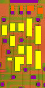
Even without the source files complete, I managed to add them to the simulation. Of course, as the chip is missing a large section, it doesn't work yet. It is a good visual demonstration of whats been digitized so far.
 |
| The simulation, note the missing area of diffusion (pink) in the upper right. |
Whats Next?
This project has been steadily progressing in my available free time since late January. As of this post, the compiler code is almost complete. I've done the painstaking task of tracing out every metal connection, transistor, and via on the chip. The tracing of the diffusion layer is about 70% complete. Once I'm done with it I'll have to debug any errors or missed components in the simulation. After the chip seems to be working, I'll need to create an interface so that I, and eventually everyone else, can view the chip's output, as well as turn various circuits on and off.
In the meantime you can comment or ask questions below. Hopefully the next post won't be too far in the future, as the simulation is close to being functional.